Toyota Venza: ECU Power Source Circuit
DESCRIPTION
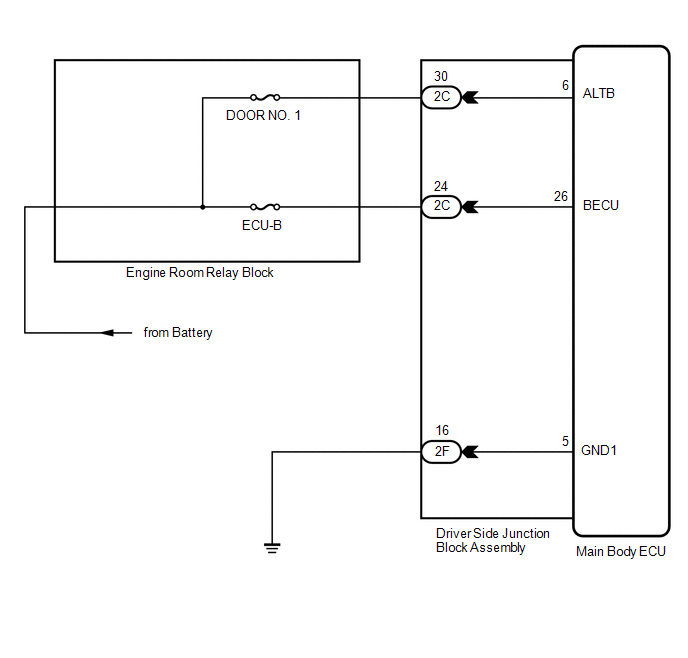
This circuit provides power for main body ECU (driver side junction block assembly) operation.
WIRING DIAGRAM
PROCEDURE
|
1. |
CHECK DRIVER SIDE JUNCTION BLOCK ASSEMBLY (MAIN BODY ECU (POWER SOURCE)) |
|
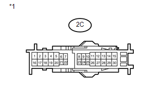
(a) Disconnect the 2C driver side junction block assembly connector. |
|
(b) Measure the voltage according to the value(s) in the table below.
Standard Voltage:
|
Tester Connection |
Condition |
Specified Condition |
|---|---|---|
|
2C-24 - Body ground |
Always |
11 to 14 V |
|
2C-30 - Body ground |
Always |
11 to 14 V |
|
*1 |
Front view of wire harness connector (to Driver Side Junction Block Assembly) |
| NG | .gif) |
REPAIR OR REPLACE HARNESS OR CONNECTOR |
|
.gif)
|
2. |
CHECK HARNESS AND CONNECTOR (DRIVER SIDE JUNCTION BLOCK ASSEMBLY - BODY GROUND) |
|
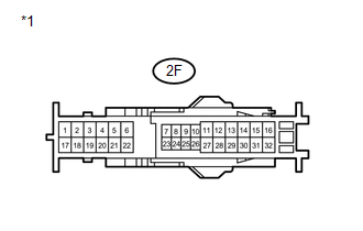
(a) Disconnect the 2F driver side junction block assembly connectors. |
|
(b) Measure the resistance according to the value(s) in the table below.
Standard Resistance:
|
Tester Connection |
Condition |
Specified Condition |
|---|---|---|
|
2F-16 - Body ground |
Always |
Below 1 Ω |
|
*1 |
Front view of wire harness connector (to Driver Side Junction Block Assembly) |
| OK | |
PROCEED TO NEXT SUSPECTED AREA SHOWN IN PROBLEM SYMPTOMS TABLE |
| NG | |
REPAIR OR REPLACE HARNESS OR CONNECTOR |
 Security Indicator Light Circuit
DESCRIPTION
Even when the theft deterrent system is in the disarmed state, the security indicator
blinks due to a signal output from the immobiliser system. The security indicator
blinks continuo ...

Other materials about Toyota Venza:
Reassembly
REASSEMBLY
PROCEDURE
1. INSTALL TRANSFER DRIVEN PINION REAR BEARING
(a) Using SST and a press, press the transfer driven pinion rear bearing
(outer race) to the case.
SST: 09950-60010
09951-00620
SST: 09950-70010
09951-07150
NO ...
Customize Parameters
CUSTOMIZE PARAMETERS
1. CUSTOMIZING FUNCTION WITH TECHSTREAM
HINT:
The following items can be customized.
NOTICE:
When the customer requests a change in a function, first make sure that
the function can be customized.
Be sure to make a not ...
Throttle / Pedal Position Sensor / Switch "A" Circuit Malfunction (P0120-P0123,P0220,P0222,P0223,P2135)
DESCRIPTION
HINT:
These DTCs relate to the throttle position sensor.
The throttle position sensor is mounted on the throttle body, and detects the
opening angle of the throttle valve. This sensor is a non-contact type sensor. It
uses hall-effect element ...

0.1614